(China (Mainland))

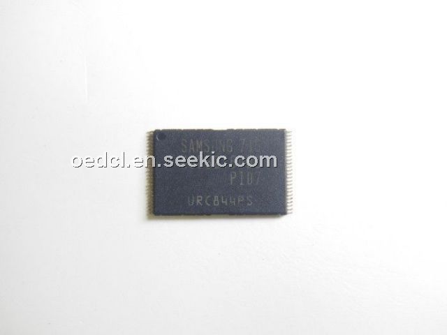
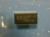
Product Summary
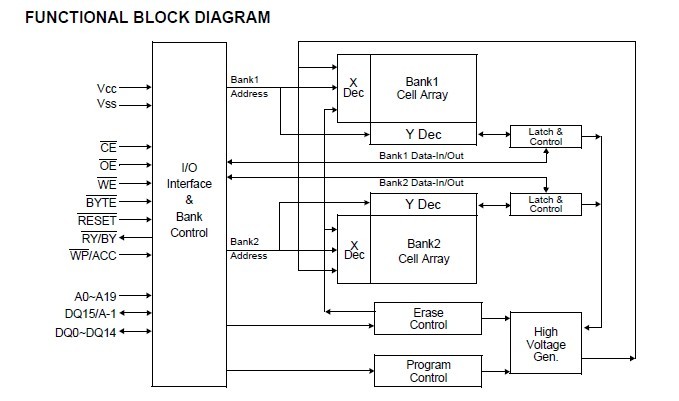
The K8D3216UBC-PI07 is a NOR Flash Memory. The K8D3216UBC-PI07 is created by using Samsungs advanced CMOS process technology. The K8D3216UBC-PI07 is available in 48 pin TSOP1 and 48 ball FBGA package. The K8D3216UBC-PI07 is compatible with EPROM applications to require highdensity and cost-effective nonvolatile read/write storage solutions. The K8D3216UBC-PI07 NOR Flash Memory is created by using Samsungs advanced CMOS process technology. The K8D3216UBC-PI07 is available in 48 pin TSOP1 and 48 ball FBGA package. The K8D3216UBC-PI07 is compatible with EPROM applications to require highdensity and cost-effective nonvolatile read/write storage solutions.
Parametrics
K8D3216UBC-PI07 absolute maximum ratings: (1)Voltage on any pin relative to VSS Vcc Vcc: -0.5 to +4.0 V; (2)A9, OE , RESET VIN: -0.5 to +12.5V; (3)WP/ACC: -0.5 to +12.5V; (4)All Other Pins: -0.5 to +4.0V; (5)Temperature Under Bias Commercial Tbias: -10 to +125 °C, Industrial: -40 to +125°C; (6)Storage Temperature Tstg: -65 to +150 °C; (7)Short Circuit Output Current IOS: 5 mA; (8)Operating Temperature TA (Commercial Temp.): 0 to +70 °C; (9)TA (Industrial Temp.): -40 to + 85 °C.
Features
K8D3216UBC-PI07 features: (1)Erase Suspend/Resume; (2)Unlock Bypass Program; (3) Hardware RESET Pin; (4)Command Register Operation; (5)Block Group Protection / Unprotection; (6)Supports Common Flash Memory Interface; (7)Industrial Temperature : - 40°C to 85°C; (8)Endurance : 100,000 Program/Erase Cycles Minimum; (9)Data Retention : 10 years; (10)Package : 48 Pin TSOP1 : 12 x 20 mm / 0.5 mm Pin pitch, 48 Ball FBGA : 6 x 8.5 mm / 0.8 mm Ball pitch, Single Voltage, 2.7V to 3.6V for Read and Write operations; (11)Organization 1,048,576 x 16 bit (Word mode); (12)Fast Read Access Time : 70ns; (13)Read While Program/Erase Operation; (14)Dual Bank architectures Bank 1 / Bank 2 : 8Mb / 8Mb; (15)Secode(Security Code)Block : Extra 64K Byte block.
Diagrams