(China (Mainland))

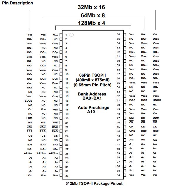
Product Summary
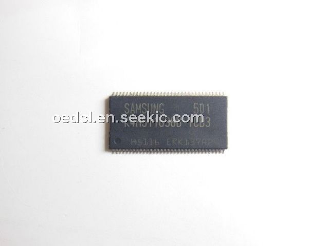
The K4H511638B-TCB3 is a 536,870,912 bits of double data rate synchronous DRAM. It is organized as 4×8,388,608 words by 16 bits, fabricated with SAMSUNG′s high performance CMOS technology. Synchronous features with Data Strobe allow extremely high performance up to 333Mb/s per pin. I/O transactions are possible on both edges of DQS. Range of operating frequencies, programmable burst length and programmable latencies allow the device to be useful for a variety of high performance memory system applications.
Parametrics
K4H511638B-TCB3 absolute maximum ratings: (1)Voltage on any pin relative to VSS: -0.5V to 3.6V; (2)Voltage on VDD & VDDQ supply relative to VSS: -1.0V to3.6V; (3)Storage temperature TSTG: -55℃ to +150 ℃; (4)Power dissipation PD: 1.5W; (5)Short circuit current IOS: 50mA.
Features
K4H511638B-TCB3 features: (1)Double-data-rate architecture; two data transfers per clock cycle; (2)Bidirectional data strobe [DQ] (×4,×8) & [L(U)DQS] (×16); (3)Four banks operation; (4)All inputs except data & DM are sampled at the positive going edge of the system clock(CK); (5)Data I/O transactions on both edges of data strobe; (6)Edge aligned data output, center aligned data input; (7)LDM,UDM for write masking only (×16); (8)DM for write masking only (×4, ×8); (9)Auto & Self refresh; (10)7.8us refresh interval(8K/64ms refresh); (11)Maximum burst refresh cycle: 8; (12)66pin TSOP II package.
Diagrams