Product Summary
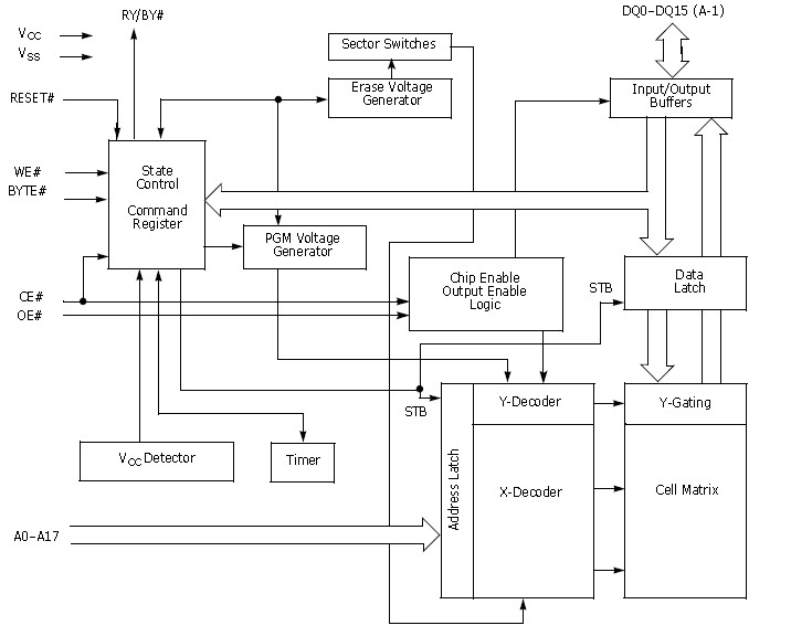
The S29AL004D70TFI01 is a 4 Mbit, 3.0 volt-only Flash memory organized as 524,288 bytes or 262,144 words. The S29AL004D70TFI01 is offered in 48-ball FBGA, 44-pin SO, and 48-pin TSOP packages. The word-wide data (x16)appears on DQ15–DQ0; the byte-wide (x8) data appears on DQ7–DQ0. The S29AL004D70TFI01 requires only a single, 3.0 volt VCC supply to perform read, program, and erase operations. A standard EPROM programmer can also be used to program and erase the device.
Parametrics
S29AL004D70TFI01 absolute maximum ratings: (1)Storage Temperature Plastic Packages : –65℃ to +150℃; (2)Ambient Temperature with Power Applied: –65℃ to +85℃; (3)Voltage with Respect to Ground VCC (Note 1): –0.5 V to +4.0 V; (4)A9, OE#, and RESET# : –0.5 V to +12.5 V; (5)All other pins : –0.5 V to VCC+0.5 V; (6)Output Short Circuit Current: 200 mA.
Features
S29AL004D70TFI01 features: (1)Single power supply operation: 2.7 to 3.6 volt read and write operations for battery-powered applications; (2)Manufactured on 200nm process technology: Compatible with 320nm Am29LV400B and MBM29LV400T/BC; (3)Flexible sector architecture: One 16 Kbyte, two 8 Kbyte, one 32 Kbyte, and seven 64 Kbyte sectors (byte mode); One 8 Kword, two 4 Kword, one 16 Kword, and seven 32 Kword sectors (word mode); Supports full chip erase; (4)Unlock Bypass Program Command: Reduces overall programming time when issuing multiple program command sequences; (5)Top or bottom boot block configurations available; (6)Embedded Algorithms: Embedded Erase algorithm automatically preprograms and erases the entire chip or any combination of designated sectors; Embedded Program algorithm automatically writes and verifies data at specified addresses; (7)Compatibility with JEDEC standards: Pinout and software compatible with single-power supply Flash; Superior inadvertent write protection; (8)Sector Protection features: A hardware method of locking a sector to prevent any program or erase operations within that sector; Sectors can be locked in-system or via programming equipment; Temporary Sector Unprotect feature allows code changes in previously locked sectors; (9)High performance: Access times as fast as 70 ns; (10)Ultra low power consumption (typical values at 5 MHz): 200 nA Automatic Sleep mode current; 200 nA standby mode current; 9 mA read current; 20 mA program/erase current; (11)Cycling Endurance: 1,000,000 cycles per sector typical; (12)Data Retention: 20 years typical; (13)Package Options: 48-ball FBGA; 48-pin TSOP; 44-pin SO ; (14)Data# Polling and toggle bits: Provides a software method of detecting program or erase operation completion; (15)Erase Suspend/Erase Resume: Suspends an erase operation to read data from, or program data to, a sector that is not being erased, then resumes the erase operation; (16)Ready/Busy# pin (RY/BY#): Provides a hardware method of detecting program or erase cycle completion; (17)Hardware reset pin (RESET#): Hardware method to reset the device to reading array data.
Diagrams

 (China (Mainland))


