Product Summary
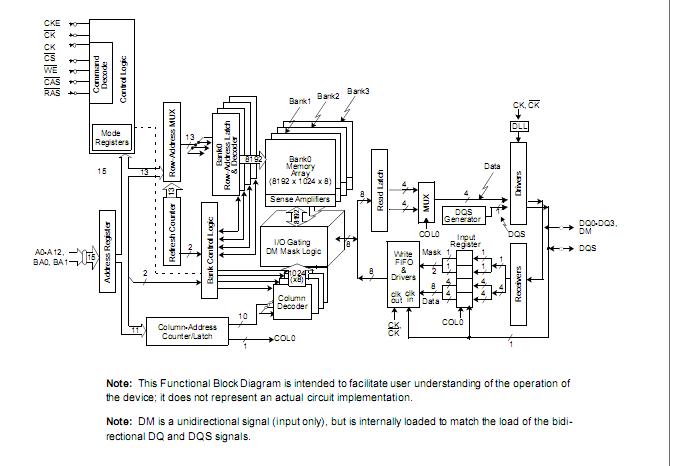
The ng5ds16m16cs-5t is a 256Mb DDR Synchronous DRAM. The ng5ds16m16cs-5t uses a double-data-rate architecture to achieve high-speed operation. The ng5ds16m16cs-5t is based on Nanya 110 nm design process. The ng5ds16m16cs-5t operates from a differential clock (CK and CK; the crossing of CK going high and CK going LOW is referred to as the positive edge of CK) . Read and write accesses to the ng5ds16m16cs-5t are burst oriented; accesses start at a selected location and continue for a programmed number of locations in a programmed sequence. The ng5ds16m16cs-5t provides for programmable Read or Write burst lengths of 2, 4, or 8 locations.
Parametrics
ng5ds16m16cs-5t absolute maximum ratings: (1) Voltage on I/O pins relative to VSS, VIN, VOUT: -0.5 to VDDQ +0.5V; (2) Voltage on Inputs relative to VSS, VIN: -0.5 to +3.6V; (3) Voltage on VDD supply relative to VSS, VDD: -0.5 to +3.6V; (4) Voltage on VDDQ supply relative to VSS, VDDQ: -0.5 to +3.6V; (5) Operating Temperature (Ambient) TA: 0 to 70°C; (6) Storage Temperature (Plastic) TSTG: -55 to 150°C; (7) Power Dissipation PD: 1W; (8) Short Circuit Output Current IOUT: 50mA.
Features
ng5ds16m16cs-5t features: (1) DDR 256M bit, die C, based on 110nm design rules; (2) Double data rate architecture: two data transfers per clock cycle; (3) Bidirectional data strobe (DQS) is transmitted and received with data, to be used in capturing data at the receiver; (4) DQS is edge-aligned with data for reads and is center-aligned with data for writes; (5) Differential clock inputs (CK and CK) ; (6) Four internal banks for concurrent operation; (7) Data mask (DM) for write data; (8) DLL aligns DQ and DQS transitions with CK transitions; (9) Commands entered on each positive CK edge; data and data mask referenced to both edges of DQS; (10) Burst lengths: 2, 4, or 8; (11) Auto Refresh and Self Refresh Modes; (12) 7.8μs Maximum Average Periodic Refresh Interval; (13) 2.5V (SSTL_2 compatible) I/O; (14) Available in Halogen and Lead Free packaging.
Diagrams

 (China (Mainland))


