(China (Mainland))

Product Summary
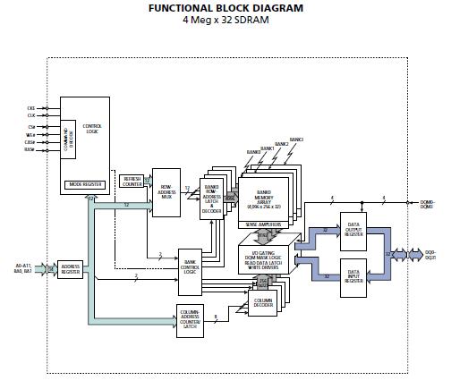
The MT48LC4M32B2TG-7G is a 128Mb SDRAM. The MT48LC4M32B2TG-7G is internally configured as a quad-bank DRAM with a synchronous interface (all signals are registered on the positive edge of the clock signal, CLK). The MT48LC4M32B2TG-7G is designed to operate in 3.3V, low-power memory systems. An auto refresh mode is provided, along with a power-saving, power-down mode. All inputs and outputs are LVTTL-compatible. SDRAMs offer substantial advances in DRAM operating performance, including the ability to synchronously burst data at a high data rate with automatic column-address generation, the ability to interleave between internal banks to hide precharge time and the capability to randomly change column addresses on each clock cycle during a burst access.
Parametrics
MT48LC4M32B2TG-7G absolute maximum ratings: (1)Voltage on VDD, VDDQ Supply Relative to VSS: -1V to +4.6V; (2)Voltage on Inputs, NC or I/O Pins Relative to VSS: -1V to +4.6V; (3)Operating Temperature, TA: 0℃ to +70℃; (4)Storage Temperature (plastic): -55℃ to +150℃; (5)Power Dissipation: 1W; (6)Operating Temperature, TA (IT): -40℃ to +85℃.
Features
MT48LC4M32B2TG-7G features: (1)PC100 functionality; (2)Fully synchronous; all signals registered on positive edge of system clock; (3)Internal pipelined operation; column address can be changed every clock cycle; (4)Internal banks for hiding row access/precharge; (5)Programmable burst lengths: 1, 2, 4, 8, or full page; (6)Auto Precharge, includes CONCURRENT AUTO PRECHARGE, and Auto Refresh Modes; (7)Self Refresh Mode; (8)64ms, 4,096-cycle refresh (15.6μs/row); (9)LVTTL-compatible inputs and outputs; (10)Single +3.3V ±0.3V power supply; (11)Supports CAS latency of 1, 2, and 3.
Diagrams