(China (Mainland))

Product Summary
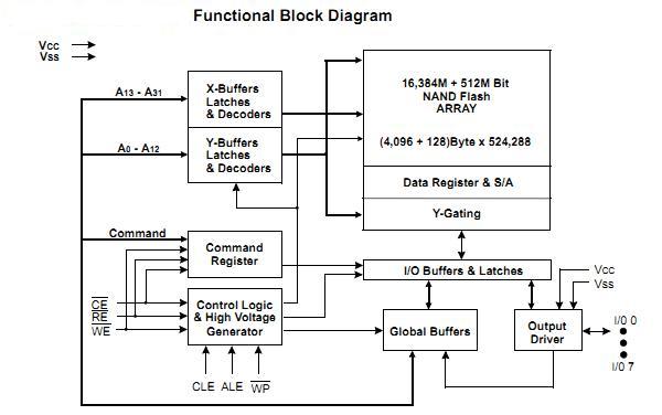
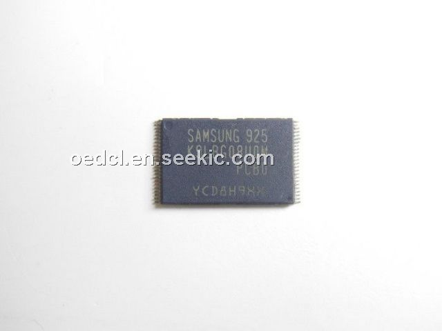
The K9LBG08U0M-PCB0 is a 16,896Mbit(17,716,740,096 bit) memory organized as 524,288 rows(pages) by 4,224x8 columns. The memory array of the K9LBG08U0M-PCB0 is made up of 32 cells that are serially connected to form a NAND structure. Each of the 32 cells resides K9LBG08U0M-PCB0 in a different page. The program and read operations are executed on a page basis, while the erase operation is executed on a block basis. The memory array of the K9LBG08U0M-PCB0 consists of 4,096 separately erasable 512K-byte blocks.
Parametrics
K9LBG08U0M-PCB0 absolute maximum ratings: (1)Voltage on any pin relative to VSS, VCC: -0.6 to + 4.6V; VIN: -0.6 to + 4.6V; VI/O: -0.6 to Vcc+0.3 (<4.6V); (2)Temperature Under Bias, TBIAS: -10 to +125℃; (3)Storage Temperature, TSTG: -65 to +150℃; (4)Short Circuit Current, Ios: 5 mA.
Features
K9LBG08U0M-PCB0 features: (1)Voltage Supply: 2.5V to 2.9V; (2)Organization: Memory Cell Array: (2G + 64M) x 8bit; Data Register: (4K + 128) x 8bit; (3)Automatic Program and Erase: Page Program: (4K + 128)Byte; Block Erase: (512K + 16K)Byte; (4)Page Read Operation: Page Size: (4K + 128)Byte; Random Read: 60μs(Max.); Serial Access: 25ns(Min.); (5)Memory Cell: 2bit / Memory Cell; (6)Fast Write Cycle Time: Program time: 800μs(Typ.); Block Erase Time: 1.5ms(Typ.); (7)Command/Address/Data Multiplexed I/O Port; (8)Hardware Data Protection: Program/Erase Lockout During Power Transitions.
Diagrams