(China (Mainland))

Product Summary
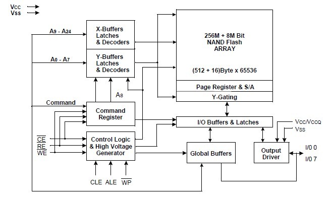
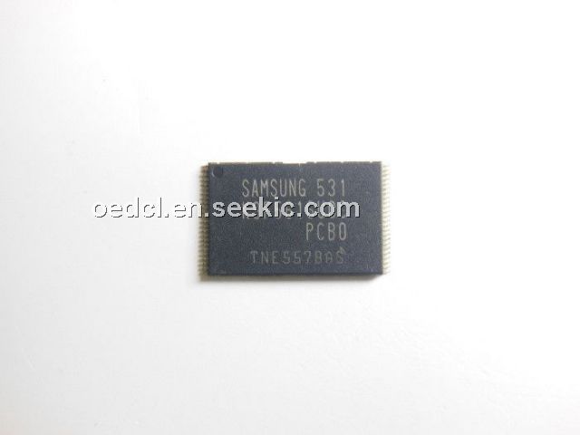
The K9F5616U0C-PCB0 is an NAND Flash Errata. Offered in 32Mx8bit or 16Mx16bit, the K9F5616U0C-PCB0 is 256M bit with spare 8M bit capacity. The K9F5616U0C-PCB0 is offered in 1.8V or 3.3V Vcc. Its NAND cell provides the most cost-effective solutIon for the solid state mass storage market. A program operation can be performed in typical 200ms on a 528-byte(X8 device) or 264-word(X16 device) page and an erase operation can be performed in typical 2ms on a 16K-byte(X8 device) or 8K-word(X16 device) block. Data in the page can be read out at 50ns cycle time per word. The I/O pins serve as the ports for address and data input/output as well as command input. The on-chip write control automates all program and erase functions including pulse repetition, where required, and internal verification and margining of data.
Parametrics
K9F5616U0C-PCB0 absolute maximum ratings: (1)Voltage on any pin relative to VSS; (2)VIN/OUT: -0.6 to + 4.6V; (3)VCC: -0.6 to + 4.6 V; (4)VCCQ: -0.6 to + 4.6V; (5)Temperature Under Bias TBIAS: -10 to +125 °C; (6)Storage Temperature TSTG: -65 to +150 °C; (7)Short Circuit Current Ios: 5 mA.
Features
K9F5616U0C-PCB0 features: (1)Fast Write Cycle Time: Program time : 200ms(Typ.), Block Erase Time : 2ms(Typ.); (2)Command/Address/Data Multiplexed I/O Port; (3)Hardware Data Protection: Program/Erase Lockout During Power Transitions; (4)Reliable CMOS Floating-Gate Technology: Endurance : 100K Program/Erase Cycles, Data Retention : 10 Years; (5)Command Register Operation; (6)Intelligent Copy-Back; (7)Unique ID for Copyright Protection; (8)Power-On Auto-Read Operation; (9)Safe Lock Mechanism.
Diagrams