(China (Mainland))

Product Summary
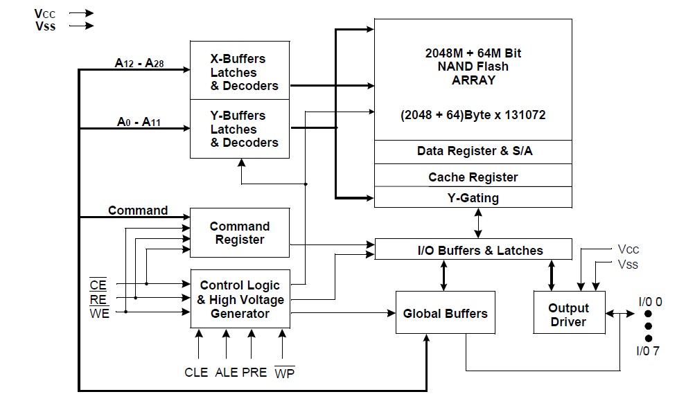
The K9F2G08U0M-PCBO is a flash memory. The K9F2G08U0M-PCBO is 2G bit with spare 64M bit capacity. The K9F2G08U0M-PCBO NAND cell provides the most costeffective solution for the solid state mass storage market. A program operation can be performed in typical 300ms on the 2112-byte(X8 device) or 1056-word(X16 device) page and an erase operation can be performed in typical 2ms on a 128K-byte(X8 device) or 64K-word(X16 device) block. Data in the data page can be read out at 50ns(30ns, only X8 device) cycle time per byte or word(X16 device). The K9F2G08U0M-PCBO I/O pins serve as the ports for address and data input/output as well as command input. The on-chip write controller automates all program and erase functions including pulse repetition, where required, and internal verification and margining of data.
Parametrics
K9F2G08U0M-PCBO absolute maximum ratings: (1)Voltage on any pin relative to VSS, VIN/OUT: -0.6 to + 4.6V; (2)VCC: -0.6 to + 4.6V; (3)Temperature Under Bias, TBIAS: -10 to +125℃; (4)Storage Temperature, TSTG: -65 to +150℃; (5)Short Circuit Current, Ios: 5 mA.
Features
K9F2G08U0M-PCBO features: (1)Voltage supply, 3.3V device: 2.7 V ~3.6 V; (2)Organization, memory cell array, X8 device(K9F2G08X0M): (256M + 8,192K)bit x 8bit; (3)Data register, X8 device(K9F2G08X0M): (2K + 64)bit x8bit; (4)Cache register: X8 device(K9F2G08X0M) : (2K + 64)bit x8bit; (5)Automatic program and erase, page program, X8 device(K9F2G08X0M) : (2K + 64)Byte; (6)Block erase, X8 device(K9F2G08X0M) : (128K + 4K)Byte; (7)Command/Address/Data Multiplexed I/O port; (8)Command register operation; (9)Cache program operation for high performance program; (10)Power-on auto-read operation; (11)Intelligent copy-back operation; (12)Unique ID for copyright protection.
Diagrams