(China (Mainland))

Product Summary
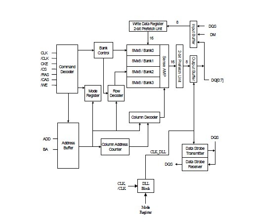
The HY5DU56822ETP-J is a DDR SDRAM. The HY5DU56822ETP-J is ideally suited for main memory applications which requires large memory density and high bandwidth. The HY5DU56822ETP-J offers fully synchronous operations referenced to both rising and falling edges of the clock. While all addresses and control inputs are latched on the rising edges of the CK (falling edges of the /CK), Data, Data strobes and Write data masks inputs are sampled on both rising and falling edges of it. The data paths are internally pipelined and 2-bit prefetched to achieve very high bandwidth. All input and output voltage levels are compatible with SSTL_2.
Parametrics
HY5DU56822ETP-J absolute maximum ratings: (1)Operating Temperature (Ambient)TA: 0 to 70 °C; (2)Storage Temperature TSTG: -55 to 150 °C; (3)Voltage on VDD relative to VSS VDD: -1.0 to 3.6 V; (4)Voltage on VDDQ relative to VSS VDDQ: -1.0 to 3.6 V; (5)Voltage on inputs relative to VSS VINPUT: -1.0 to 3.6 V; (6)Voltage on I/O pins relative to VSS VIO: -0.5 to 3.6 V; (7)Output Short Circuit Current IOS: 50 mA.
Features
HY5DU56822ETP-J features: (1)All addresses and control inputs except data, data strobes and data masks latched on the rising edges of the clock; (2)Programmable CAS latency 2/2.5 (DDR200, 266, 333)and 3 (DDR400)supported; (3)Programmable burst length 2/4/8 with both sequential and interleave mode; (4)Internal four bank operations with single pulsed /RAS; (5)Auto refresh and self refresh supported; (6)tRAS lock out function supported; (7)8192 refresh cycles / 64ms; (8)60 Ball FBGA Package Type; (9)Full and Half strength driver option controlled by EMRS; (10)Lead free (ROHS Compliant).
Diagrams