Product Summary
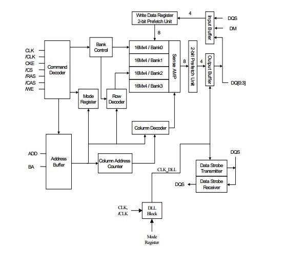
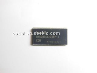
The Hynix HY5DU56822DTP-J is a 268,435,456-bit CMOS Double Data Rate(DDR) Synchronous DRAM, ideally suited for the main memory applications which requires large memory density and high bandwidth. The Hynix 256Mb DDR SDRAM HY5DU56822DTP-J offers fully synchronous operations referenced to both rising and falling edges of the clock. While all addresses and control inputs are latched on the rising edges of the CK (falling edges of the /CK), Data, Data strobes and Write data masks inputs are sampled on both rising and falling edges of it.
Parametrics
HY5DU56822DTP-J absolute maximum ratings: (1)Ambient Temperature: TA: 0 ~ 70°C; (2)Storage Temperature: TSTG: -55 ~ 125°C; (3)Voltage on Any Pin relative to VSS: VIN, VOUT: -0.5 ~ 3.6 V; (4)Voltage on VDD relative to VSS: VDD: -0.5 ~ 3.6 V; (5)Voltage on VDDQ relative to VSS: VDDQ: -0.5 ~ 3.6 V; (6)Output Short Circuit Current: IOS: 50 mA; (7)Power Dissipation: PD: 1 W; (8)Soldering Temperature . Time: TSOLDER: 260. 10. sec.
Features
HY5DU56822DTP-J features: (1)VDD, VDDQ = 2.5V +/- 0.2V; (2)All inputs and outputs are compatible with SSTL_2 interface; (3)Fully differential clock inputs (CK, /CK)operation; (4)Double data rate interface; (5)Source synchronous - data transaction aligned to bidirectional data strobe (DQS); (6)x16 device has two bytewide data strobes (UDQS, LDQS)per each x8 I/O; (7)Data outputs on DQS edges when read (edged DQ); (8)Data inputs on DQS centers when write (centered DQ); (9)On chip DLL align DQ and DQS transition with CK transition; (10)DM mask write data-in at the both rising and falling edges of the data strobe.
Diagrams

 (China (Mainland))


