(China (Mainland))

Product Summary
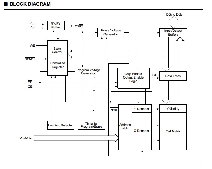
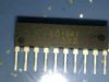
The 29F080A-90PFTN is an 8 M-bit, 5.0 V-Only Flash memory organized as 1 M bytes of 8 bits each. The 1 M bytes of data is divided into 16 sectors of 64 K bytes for flexible erase capability. The 8 bit of data will appear on DQ0 to DQ7. The 29F080A-90PFTN is offered in a 48-pin TSOP(I), 40-pin TSOP, and 44-pin SOP packages. This device is designed to be programmed in-system with the standard system 5.0 V VCC supply. A 12.0 V VPP is not required for program or erase operations. The 29F080A-90PFTN can also be reprogrammed in standard EPROM programmers.
Parametrics
29F080A-90PFTN absolute maximum ratings: (1)Storage Temperature: Tstg: −55 to +125 °C; (2)Ambient Temperature with Power Applied: TA: −40 to +85 °C; (3)Voltage with Respect to Ground All pins except A9, OE, and RESET:−2.0 to +7.0 V; (4)Power Supply Voltage:−2.0 to +7.0 V; (5)A9, OE, and RESET: −2.0 to +13.5 V.
Features
29F080A-90PFTN features: (1)Single 5.0 V read, write, and erase Minimizes system level power requirements; (2)Compatible with JEDEC-standard commands Pinout and software compatible with single-power supply Flash Superior inadvertent write protection; (3)48-pin TSOP(I)(Package Suffix: PFTN-Normal Bend Type, PFTR-Reverse Bend Type); (4)40-pin TSOP(I)(Package Suffix: PTN-Normal Bend Type, PTR-Reversed Bend Type); (5)44-pin SOP (Package Suffix: PF); (6)Minimum 100,000 write/erase cycles; (7)High performance 55 ns maximum access time; (8)Sector erase architecture Uniform sectors of 64 K bytes each; (9)Any combination of sectors can be erased. Also supports full chip erase.; (10)Embedded Erase Algorithms, Automatically pre-programs and erases the chip or any sector; (11)Embedded Program Algorithms, Automatically programs and verifies data at specified address; (12)Data Polling and Toggle Bit feature for detection of program or erase cycle completion.
Diagrams