(China (Mainland))

Product Summary
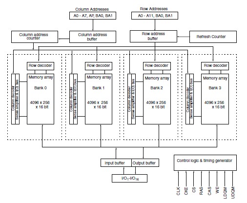
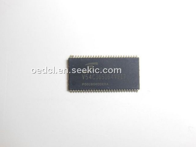
The V54C365164VE17 is a four bank synchronous DRAM organized as 4 banks x 1Mbit x 16. The V54C365164VE17 achieves high speed data transfer rates up to 166 MHz by employing a chip architecture that prefetches multiple bits and then synchronizes the output data to a system clock all of the control, address, data input and output circuits are synchronized with the positive edge of an externally supplied clock. Operating the four memory banks in an interleaved fashion allows random access operation to occur at higher rate than is possible with standard DRAMs. A sequential and gapless data rate of up to 166 MHz is possible depending on burst length, CAS latency and speed grade of the device.
Parametrics
V54C365164VE17 absolute maximum ratings: (1)Operating temperature range: 0 to 70 °C; (2)Storage temperature range: -55 to 150 °C; (3)Input/output voltage: -0.3 to (VCC+0.3)V; (4)Power supply voltage: -0.3 to 4.6 V; (5)Power dissipation: 1 W; (6)Data out current (short circuit): 50 mA.
Features
V54C365164VE17 features: (1)4 banks x 1Mbit x 16 organization; (2)High speed data transfer rates up to 166 MHz; (3)Full synchronous dynamic RAM, with all signals referenced to clock rising edge; (4)Single pulsed RAS interface; (5)Data mask for byte control; (6)Four banks controlled by BA0 & BA1; (7)Programmable CAS latency: 1, 2, & 3; (8)Programmable wrap sequence: Sequential or interleave; (9)Programmable burst length: 1, 2, 4, 8 and full page for sequential Type; 1, 2, 4, 8 for interleave Type; (10)Multiple burst read with single write operation; (11)Automatic and controlled precharge command; (12)Random column address every CLK (1-N Rule); (13)Suspend mode and power down mode; (14)Auto refresh and self refresh; (15)Refresh interval: 4096 cycles/64 ms; (16)Available in 54 Pin 400 mil TSOP-II; (17)LVTTL interface; (18)Single +3.3 V ± 0.3 V power supply.
Diagrams