(China (Mainland))

Product Summary
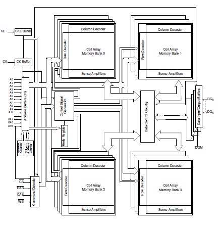
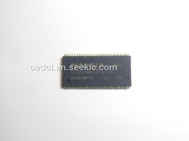
The NT5SV8M16FS-6K is a four-bank synchronous DRAM. It is organized as 2Mbit x 16 I/O x 4 bank. The NT5SV8M16FS-6K achieves high-speed data transfer rates of up to 166MHz by employing a pipeline chip architecture that synchronizes the output data to a system clock. The NT5SV8M16FS-6K is designed to comply with all JEDEC standards set for synchronous DRAM products, both electrically and mechanically. All of the control, address, and data input/output (I/O or DQ) circuits are synchronized with the positive edge of an externally supplied clock.
Parametrics
NT5SV8M16FS-6K absolute maximum ratings: (1)VDD Power supply voltage: -1.0 to +4.6 V; (2)VDDQ power supply voltage for output: -1.0 to +4.6 V; (3)VIN input voltage: -0.3 to VDD+0.3 V; (4)VOUT output voltage: -0.3 to VDD+0.3 V; (5)TA operating temperature (ambient)commerical: 0 to +70 ℃, industrial: -40 to +85 ℃; (6)TSTG storage temperature: -55 to +150 ℃; (7)PD power dissipation: 1.0 W; (8)IOUT short circuit output current: 50 mA.
Features
NT5SV8M16FS-6K features: (1)Single pulsed RAS interface; (2)Fully synchronous to positive clock edge; (3)Four banks controlled by BA0/BA1 (bank select); (4)Programmable CAS latency: 2, 3; (5)Programmable burst length: 1, 2, 4, 8 or full page; (6)Programmable Wrap: Sequential or Interleave; (7)Multiple burst read with single write option; (8)Automatic and controlled precharge command; (9)Dual data mask for byte control (×16); (10)Auto refresh (CBR) and self refresh; (11)Suspend mode and power down mode; (12)Standard power operation; (13)Random column address every CK (1-N Rule); (14)Single power supply, either 3.3V; (15)LVTTL compatible; (16)Packages: TSOP-Type II; (17)Lead-free, Halogen-free product available.
Diagrams