(China (Mainland))

Product Summary
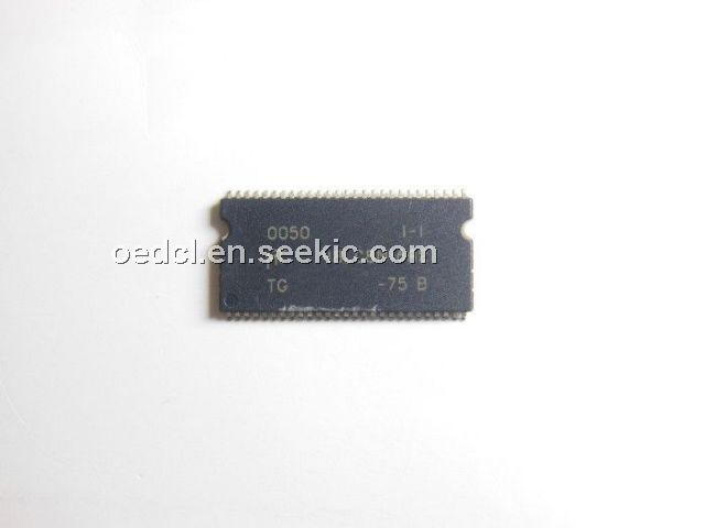
The MT48LC8M16A2TG-75B is a quad-bank DRAM that operates at 3.3V and includes a synchronous interface (all signals are registered on the positive edge of the clock signal, CLK). Read and write accesses to the MT48LC8M16A2TG-75B are burst oriented; accesses start at a selected location and continue for a programmed number of locations in a programmed sequence. It uses an internal pipelined architecture to achieve high-speed operation. This architecture is compatible with the 2n rule of prefetch architectures, but the MT48LC8M16A2TG-75B also allows the column address to be changed on every clock cycle to achieve a high-speed, fully random access.
Parametrics
MT48LC8M16A2TG-75B absolute maximum ratings: (1)Voltage on VDD, VDDQ supply relative to VSS:–1V to +4.6V; (2)Voltage on inputs, NC or I/O pins relative to VSS: –1V to +4.6V; (3)Operating temperature: TA (commercial):0℃ to 70℃, TA (extended; IT parts):-40℃ to +85℃; (4)Storage temperature (plastic):-55℃ to +150℃; (5)Power dissipation: 1W.
Features
MT48LC8M16A2TG-75B features:(1)PC100-compliant;includes concurrent auto precharge; (2)fully synchronous, all signals registered on positive edge of system clock; (3)internal pipelined operation, column address can be changed every clock cycle; (4)internal banks for hiding row access / precharge; (5)programmable burst lengths:1,2,4,8 or full page; (6)auto precharge and auto refresh modes; (7)self refresh mode; (8)64 ms, 4,096-cycle refresh; (9)single +3.3V+/-0.3V power supply; (10)one and two clock write recovery versions.
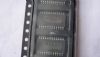
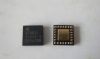
Diagrams