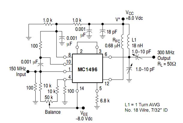
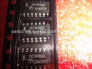
Product Summary
The mc1496d is a balanced modulator/demodulator. The mc1496d is designed for use where the output voltage is a product of an input voltage (signal) and a switching function (carrier) . Typical applications of the mc1496d include suppressed carrier and amplitude modulation, synchronous detection, FM detection, phase detection, and chopper applications.
Parametrics
mc1496d absolute maximum ratings: (1) Applied Voltage Applied Voltage (V6-V8, V10-V1, V12-V8, V12-V10, V8-V4, V8-V1, V10-V4, V6-V10, V2-V5, V3-V5) V: 30V; (2) Differential Input Signal V8-V10: +5V, V4-V1: ±(5+I5Re) V; (3) Maximum Bias Current I5: 10mA; (4) Thermal Resistance, Junction-to-Air Plastic Dual In-Line Package RθJA: 100°C/W; (5) Operating Ambient Temperature Range TA: 0 to 70°C; (6) Storage Temperature Range Tstg: -65 to +150°C; (7) Electrostatic Discharge Sensitivity (ESD) Human Body Model (HBM) : 2000V.
Features
mc1496d features: (1) Excellent Carrier Suppression -65dB typ@0.5MHz, -50dB typ@10 MHz; (2) Adjustable Gain and Signal Handling; (3) Balanced Inputs and Outputs; (4) High Common Mode Rejection -85dB Typical; (5) This Device Contains 8 Active Transistors; (6) Pb-Free Package is Available.
Diagrams

| Image | Part No | Mfg | Description |  |
Pricing (USD) |
Quantity | ||||||||||||
|---|---|---|---|---|---|---|---|---|---|---|---|---|---|---|---|---|---|---|
 |
 MC1496D |
 ON Semiconductor |
 Modulator / Demodulator Balanced Mod/DeMod |
 Data Sheet |
 Negotiable |
|
||||||||||||
 |
 MC1496DG |
 ON Semiconductor |
 Modulator / Demodulator Balanced Mod/DeMod |
 Data Sheet |

|
|
||||||||||||
 |
 MC1496DR2 |
 ON Semiconductor |
 Modulator / Demodulator Balanced Mod/DeMod |
 Data Sheet |
 Negotiable |
|
||||||||||||
 |
 MC1496DR2G |
 ON Semiconductor |
 Modulator / Demodulator Balanced Mod/DeMod |
 Data Sheet |

|
|
||||||||||||
 (China (Mainland))


