Product Summary
The DS12C887 is a Real Time Clock plus RAM designed to be a direct replacement for the DS1287. The DS12C887 is identical in form, fit, and function to the DS1287, and has an additional 64 bytes of general purpose RAM. Access to this additional RAM space is determined by the logic level presented on AD6 during the address portion of an access cycle. A lithium energy source, quartz crystal, and write rotection circuitry are contained within a 24–pin dual in-line package. As such, the DS12C887 is a complete subsystem replacing 16 components in a typical application. The functions include a nonvolatile time–of–day clock, an alarm, a onehundred year calendar, programmable interrupt, square wave generator, and 114 bytes of nonvolatile static RAM. The real time clock is distinctive in that time of–day and memory are maintained even in the absence of power. The applications of the DS12C887 include Embedded Systems, Utility Meters, Security Systems and Network Hubs, Bridges, and Routers.
Parametrics
DS12C887 absolute maximum ratings: (1)Voltage Range on VCC Pin Relative to Ground: -0.3V to +6.0V; (2)Operating Temperature Range, Commercial (noncondensing): 0℃ to +70℃; (3)Operating Temperature Range, Industrial (noncondensing): -40℃ to +85℃; (4)Storage Temperature Range, EDIP: -40℃ to +85℃; (5)PDIP, SO, PLCC, TQFP: -55℃ to +125℃; (6)Lead Temperature (soldering, 10s): +260℃.
Features
DS12C887 features: (1)Drop-in replacement for IBM AT computer clock/calendar; (2)Pin compatible with the MC146818B and DS1287A; (3)Totally nonvolatile with over 10 years of operation in the absence of power; (4)Self-contained subsystem includes lithium, quartz, and support circuitry; (5)Counts seconds, minutes, hours, days, day of the week, date, month, and year with leapyear compensation valid up to 2100; (6)Binary or BCD representation of time, calendar, and alarm; (7)12-hour or 24-hour clock with AM and PM in 12-hour mode; (8)Daylight Savings Time option; (9)Selectable between Motorola and Intel bus timing; (10)Multiplex bus for pin efficiency; (11)Interfaced with software as 128 RAM locations: 14 bytes of clock and control registers; 114 bytes of general-purpose RAM; (12)Programmable square-wave output signal.
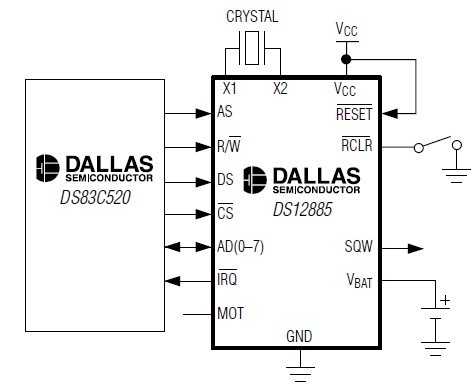
Diagrams
| Image | Part No | Mfg | Description |  |
Pricing (USD) |
Quantity | ||||||||||||
|---|---|---|---|---|---|---|---|---|---|---|---|---|---|---|---|---|---|---|
 |
 DS12C887 |
 Maxim Integrated Products |
 Real Time Clock |
 Data Sheet |
 Negotiable |
|
||||||||||||
 |
 DS12C887+ |
 Maxim Integrated Products |
 Real Time Clock RTC |
 Data Sheet |

|
|
||||||||||||
 |
 DS12C887A+ |
 Maxim Integrated Products |
 Real Time Clock RTC |
 Data Sheet |

|
|
||||||||||||
 |
 DS12C887A |
 Maxim Integrated Products |
 Real Time Clock |
 Data Sheet |
 Negotiable |
|
||||||||||||
 (China (Mainland))


