(China (Mainland))

Product Summary
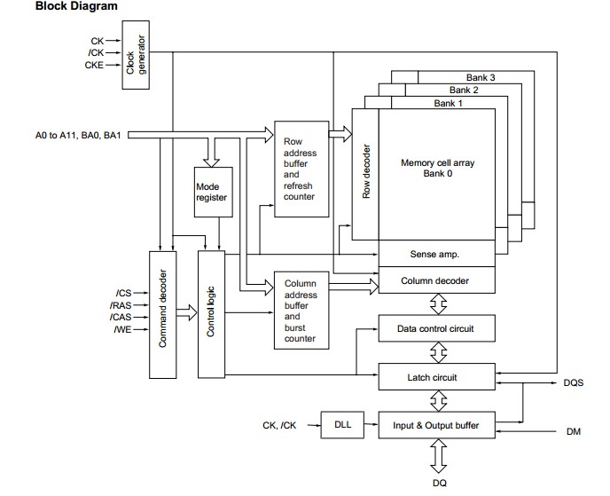
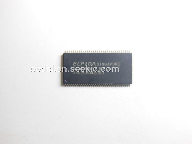
The D1216AATA-6B-E is a 128M bits Double Data Rate (DDR) SDRAM organized as 2,097,154 words × 16 bits × 4 banks. Read and write operations are performed at the cross points of the CK and the /CK. This highspeed data transfer is realized by the 2 bits prefetchpipelined architecture. Data strobe (DQS) both for read and write are available for high speed and reliable data bus design. By setting extended mode register, the on-chip Delay Locked Loop (DLL) can be set enable or disable. The D1216AATA-6B-E is packaged in 66-pin plastic TSOP (II).
Parametrics
D1216AATA-6B-E absolute maximum ratings: (1)Voltage on any pin relative to VSS: VT: –1.0 to +3.6 V; (2)Supply voltage relative to VSS: VDD: –1.0 to +3.6 V; (3)Short circuit output current: IOS: 50 mA; (4)Power dissipation: PD: 1.0 W; (5)Operating ambient temperature: TA: 0 to +70 °C; (6)Storage temperature: Tstg: –55 to +125 °C .
Features
D1216AATA-6B-E features: (1)Power supply : VDD ,VDDQ = 2.5V ± 0.2V; (2)Data rate: 333Mbps/266Mbps (max.); (3)Double Data Rate architecture; two data transfers per clock cycle; (4)Bi-directional, data strobe (DQS)is transmitted /received with data, to be used in capturing data at the receiver; (5)Data inputs, outputs, and DM are synchronized with DQS; (6)4 internal banks for concurrent operation; (7)DQS is edge aligned with data for READs; center aligned with data for WRITEs; (8)Differential clock inputs (CK and /CK); (9)DLL aligns DQ and DQS transitions with CK transitions; (10)Commands entered on each positive CK edge; data and data mask referenced to both edges of DQS; (11)Data mask (DM)for write data; (12)Auto precharge option for each burst access; (13)SSTL_2 compatible I/O; (14)Programmable burst length (BL): 2, 4, 8; (15)Programmable /CAS latency (CL): 2, 2.5; (16)Programmable output driver strength: normal/weak; (17)Refresh cycles: 4096 refresh cycles/64ms.
Diagrams